AI in Chip Design — What Actually Works, What's Marketing, and Who Should Worry
Learn In Depth · Digital Design / EDA · Deep Dive · July 2026
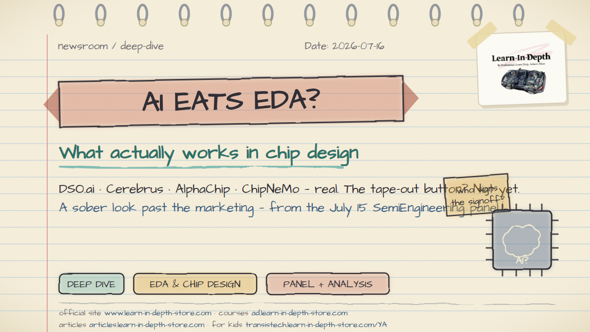
Picture this: it's 2 AM. A physical design engineer is staring at her 47th congestion heatmap of the night, coaxing a stubborn block toward timing closure. Her phone lights up with a headline: "AI now designs chips."
If that were true, why is she still awake?
On July 15, SemiEngineering published a panel discussion with a title that says the quiet part out loud: "AI In Chip Design: Lots Of Promise, Plenty Of Unanswered Questions." On stage: the CEOs and VPs of AI-EDA startups — ChipAgents, Breker, Moores Lab AI, Verific — and industry legend Wally Rhines. Conspicuously absent from the panel: Synopsys, Cadence, and Siemens EDA, the three companies that sell almost every tool your flow runs on.
Both facts — the promise and the absence — are the story. Let's take it apart, piece by piece.
SectionThe Blueprint
- The panel that said the quiet part out loud
- The question cascade
- Where AI already ships — the proven layer
- The mechanism: why AI fits some stages and not others
- The fake-out: "so, one-button tape-out?"
- The data problem nobody can solve with money
- The speed war: weekly releases vs. 12-month cycles
- Who wins, who loses — and the ladder problem
- The synthesis
Section1. The panel
The SemiEngineering discussion is refreshingly honest for a field drowning in "AI-powered" press releases. The panelists — people selling AI for chip design — spent much of the session listing what their own technology cannot yet do:
- No push-button tape-out. Despite years of industry claims, "one-button-click tape-out remains theoretical."
- Hallucinations persist. General-purpose LLMs "lack semiconductor expertise; human supervision remains essential." As Shelly Henry (Moores Lab AI) put it: "We still need semiconductor expert knowledge to say whether whatever is being done by AI is correct or not."
- The accountability void. Cindy Cui (ChipAgents) asked the question that should be printed on every AI-EDA brochure: "If we have AI controlling the entire chip design by itself, where's the accountability?"
⚠️ Honesty box: this panel represents the startup perspective — the big three EDA vendors weren't on stage (they ship their own AI, which we cover in section 3). Panel claims are quoted from SemiEngineering's July 15 report; the background on commercial tools below is from vendor publications and public research.
Section2. The question cascade
So which is it? Is AI designing chips, or not? If Google used RL to floorplan its TPUs, why does your team still fight congestion by hand? If AI can write RTL, why do verification schedules keep growing? And the question under all of them: when a black box makes a mistake that reaches silicon — who signs?
Hold that last one. We'll come back to it, because a respin at 2nm is not an "undo" — it's a seven-figure mask set and a quarter of lost market.
Section3. Where AI already ships
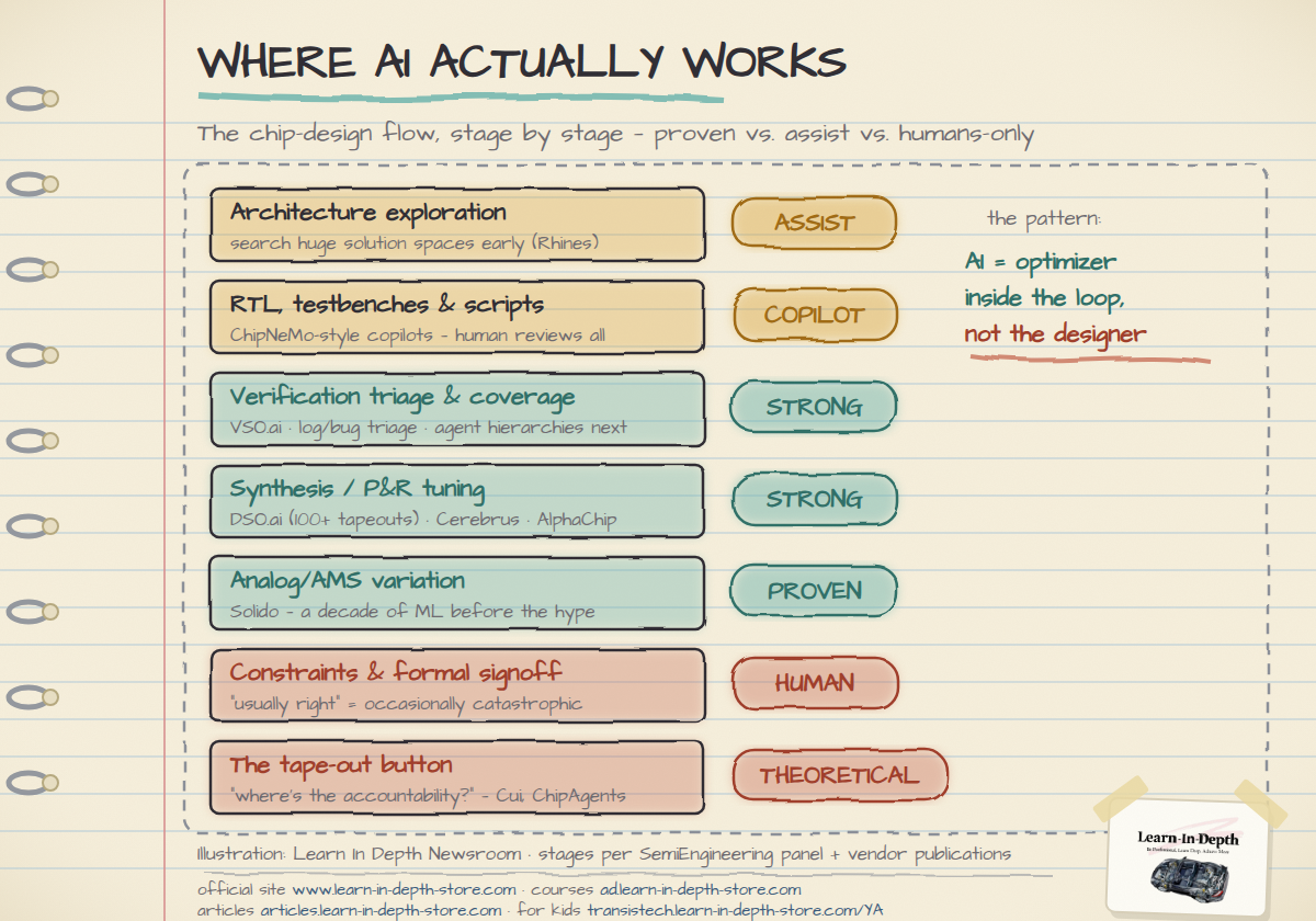
Strip the marketing, and there IS a real, proven layer — AI as an optimizer inside loops that engineers already run:
- Synopsys DSO.ai — reinforcement learning that explores the PPA solution space (floorplan, clocking, flow parameters). Launched 2020; Synopsys announced its 100th commercial tape-out in 2023, and it's now part of the broader Synopsys.ai suite (with VSO.ai for verification and TSO.ai for test).
- Cadence Cerebrus — the same idea for the Cadence flow: an RL agent that tunes implementation recipes across blocks, with reported double-digit PPA gains and big cuts in engineer-hours.
- Google AlphaChip — DeepMind's RL floorplanner, used in multiple TPU generations (published in Nature, methods openly debated in the community — and that debate itself tells you how young this field is).
- NVIDIA ChipNeMo — a domain-adapted LLM trained on internal design data: an engineering copilot for bug triage, scripting, and answering "how does this block work?" questions.
- Siemens EDA — Solido has used machine learning for variation-aware analog/mixed-signal verification for over a decade (long before the hype), and Aprisa AI brings ML-driven optimization to digital implementation.
Notice the pattern, because it's the whole thesis: every shipping success is AI optimizing within a flow that deterministic tools and human engineers still own. Nothing on this list "designs a chip." Everything on this list makes a specific loop converge faster.
(And notice something else: the big three weren't on that startup panel — but they're not asleep. They own the shipping AI. Keep that for section 8.)
Section4. The mechanism
Put on the engineering hat. Why does AI crush these problems and stumble elsewhere?
Where RL fits: floorplanning and P&R tuning are gigantic search spaces with a cheap, computable reward — run the flow, read PPA, adjust. That's the same shape as a game: huge state space, scoreboard at the end. RL eats that shape (AlphaGo → AlphaChip is a straight line).
Where LLMs fit: language-shaped work — testbench scaffolding, assertions, tool scripts, documentation lookup, log triage. ChipNeMo-style copilots work because the cost of a wrong suggestion is low: a human reviews before anything matters.
Where both stall: stages whose output must be provably correct, not statistically good. Constraints. Formal signoff. LVS/DRC interpretation for a specific foundry's rule deck under NDA. There, "usually right" is another way of saying "occasionally catastrophic."
💡 Engineer's mental model: AI in today's flow is an autopilot, not a pilot. It flies the cruise phase brilliantly — millions of small corrections in a bounded space, better than any human. But takeoff decisions, landing, and signing the flight log belong to the crew. Nobody boards a plane whose autopilot also does the pre-flight inspection and signs its own airworthiness certificate.
Section5. The fake-out
Here's where you say: "Fine — but the trend line is obvious. Give it two years and the button will exist."
Sounds reasonable. But no — and the panelists themselves explain why. Three walls stand between today's optimizers and push-button silicon:
- The correctness wall. An LLM that hallucinates a README costs you a laugh. A model that hallucinates a timing constraint costs you a stepping. The failure cost is asymmetric in a way consumer AI never faces.
- The accountability wall. Cui's question has no technical answer — it's organizational. Foundries want a name on the signoff. Insurers want a liable party. "The agent did it" is not a legal entity.
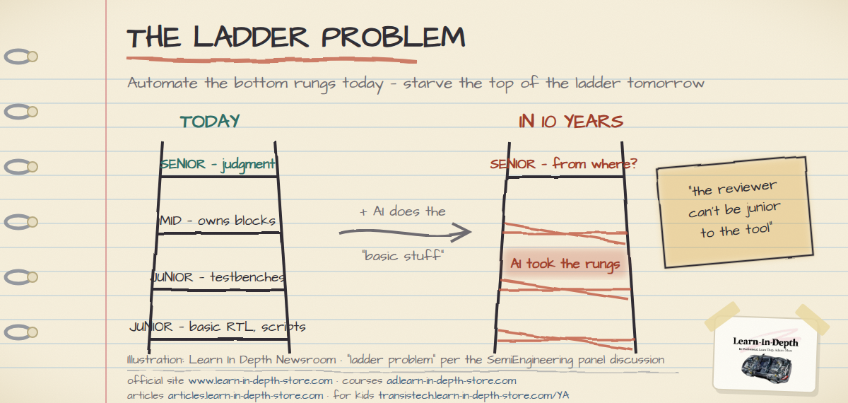
- The expertise wall. Judging AI output requires more knowledge than producing it slowly. As Dave Kelf (Breker) put it: "Engineers who are using EDA tools need to know what they are doing." The reviewer can't be junior to the tool.
Section6. The data problem
Why can't someone just train a "GPT for chip design" and be done? Because the training data is the most jealously guarded intellectual property on the planet. Real RTL, real floorplans, real signoff decks live behind foundry NDAs and trade-secret walls. Nobody pools them.
Which means domain AI belongs to whoever already owns a design corpus:
- Hyperscalers (Google, NVIDIA, Amazon, Microsoft…) train on their own silicon history — AlphaChip and ChipNeMo exist precisely because their creators own decades of designs.
- The big three EDA vendors sit on something even better: telemetry and flows across hundreds of customers — carefully firewalled, but structurally theirs to leverage.
- Startups bring speed but arrive data-poor: they must partner, fine-tune per customer, or stay in stages where public data suffices.
This is the quiet reason the revolution is slower than the demos: the fuel is locked in vaults, and the vault owners are not sharing.
Section7. The speed war
The startups' real weapon isn't smarter models — it's cadence. ChipAgents' Cindy Cui described shipping weekly releases, against the traditional EDA cycle of 6–12 months. In a field moving at AI speed, that's not an incremental advantage; it's a different species of company.
The panel also sketched where verification is heading: hierarchies of agents checking agents, with humans reviewing the top of the pyramid rather than every assertion. Wally Rhines framed the near-term prize more soberly: AI lets you explore a very large solution space early and discard bad architectures before they eat a quarter of schedule.
And the big three? Their absence from this panel is a classic innovator's-dilemma tableau — but don't write the obituary: they own the customer base, the signoff trust, and (section 6) the data position. The likely outcome isn't disruption or consolidation. It's both: startups set the pace, giants buy the winners.
Section8. Who wins, who loses
- Hyperscalers — biggest winners: proprietary data + custom-silicon ambitions (see our Anthropic × Samsung deep dive — the custom-chip queue and the AI-that-designs-chips story are the same story).
- The big three EDA vendors — pressured on cadence, protected by trust, data, and signoff gravity. Watch their M&A.
- AI-EDA startups — the panelists' companies: fastest guns, thinnest data. Acquisition targets in waiting.
- Senior engineers — more valuable than ever: someone must judge the black box, and judgment is now the scarce skill.
- Junior engineers — the at-risk tier. The panel was blunt: the "basic stuff" juniors traditionally cut their teeth on is exactly what gets automated first. And history is unkind to refusers — the panel invoked the Verilog/VHDL precedent: engineers who rejected HDLs became obsolete.
- The industry's own future — the sleeper risk the panel named: if AI does all the junior work, where do senior engineers come from in ten years? Automate the bottom of the ladder and you eventually starve the top. Call it the ladder problem — it deserves its own picture:
Section9. The synthesis
So what does all of this actually mean?
First: AI in chip design is real but bounded — a proven optimizer inside human-owned loops (DSO.ai, Cerebrus, AlphaChip, ChipNeMo, Solido), not a designer. Every "AI designed this chip" headline is compressing "AI tuned loops inside a flow that 200 engineers still ran."
Second: the binding constraints are not model quality — they're correctness cost, accountability, and locked-up training data. Those don't fall to the next GPT release.
Third: the competitive map is speed vs. trust: weekly-release startups vs. signoff-owning giants — expect acquisitions, not extinction.
Fourth: for the industry, the existential question isn't tape-out buttons; it's the talent ladder. Automating junior work today quietly cannibalizes senior judgment tomorrow — just when judgment becomes the product.
Fifth: for you personally — the winning move is neither resisting nor surrendering. Use the optimizers, keep the understanding. The engineer who can explain why the AI's answer is wrong is the most employable person in this industry for the next decade.
And the question I leave you with: when the first AI-signed-off chip fails in the field — and one day, one will — whose name ends up on the incident report: the engineer who trusted the tool, the vendor who sold it, or nobody at all? And which of those three answers scares you most?
Sources
- SemiEngineering — AI In Chip Design: Lots Of Promise, Plenty Of Unanswered Questions (July 15, 2026)
- Synopsys.ai — DSO.ai and the 100th commercial tape-out
- Cadence — Cerebrus Intelligent Chip Explorer
- Google DeepMind — How AlphaChip transformed computer chip design
- NVIDIA Research — ChipNeMo: Domain-Adapted LLMs for Chip Design
- Siemens EDA — Solido Design Environment · Aprisa AI
Written by the Learn In Depth Newsroom. Panel positions are quoted from SemiEngineering's July 15, 2026 report; commercial tool history is from vendor publications and public research as of July 16, 2026.
<div align="center"> <img src="https://static.wixstatic.com/media/2f2dbe_c6f38f088ec94ba99c763171430fb58d~mv2.png/v1/fill/w_240,h_194,al_c,q_85,usm_0.66_1.00_0.01,enc_avif,quality_auto/yarap.png" alt="Learn In Depth" width="120"/>
Learn In Depth — Go deep, not wide.
🌐 Official Site · 🎓 Courses · 📰 Articles · 🧒 For Kids — TransisTech
© 2026 Learn In Depth · Written by the Learn In Depth Newsroom
</div>
Comments